The world is never stagnant, it is going to be a very tedious task to understand even the already understood. It was a revolution to comprehend the wheel but the modern day automobiles are as complicated as the best “Modern art”. History of science has proved that any enigma can be solved if approached as multiple pieces of problem, from building the Great Wall of China (took over 2000 years to build) to understanding the arrangement of atoms and molecules. Avogadro’s number suggest that there are approximately 1023atoms/m3 and it is a bizarre task to study these as a whole. one other disturbing fact is that even though the universe seems to be expanding day by day it seems all that the engineering community is shouting loud “honey I shrunk the transistor”. Moore’s law formulated by Gordon Moore in 1965 suggests that the number of components per integrated chips doubles every two years in order to keep up with the processing demands. It is the very essential duty for the physicist to provide the perfect material that is small in size, electrically and thermally ambient, cost effective, strong etc. A combination of all this in a material sounds impossible if we were in still living in the silicon era, because in 2004 the wondrous kid, GRAPHENE was exfoliated for the first time.
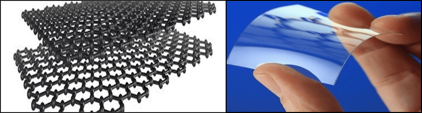
Graphene is an allotrope of carbon with a hexagonal lattice, which means one molecule has six carbon atoms arranged as in the shape of a honeycomb. This is the first fully 2D material ever made and form the building blocks for graphite with sp 2 hybridization (black, good electric conductor, soft) and diamond with sp 3 hybridization (transparent, insulator, hard), have very different physical properties. Graphene was first exfoliated mechanically (using Scotch tape!) by Dr. Andrea Geim and Dr. Konstantin Novoselvo and was awarded the Nobel Prize in 2010.This material possess the beautiful honey comb structure for its lattice which is the reason for a very high flexibility and very high strength 200 times stronger than steel. The sp2 hybridization contributes to the highest electrical conductivity, also it’s that the electronic band is in such a way that the electrical conductivity can be tuned from insulator range to conductor range that means just one material is sufficient for all the electrical works. Graphene has a 98% optical transmittance rate which means it is mostly transparent in nature, Samsung has taken up the idea of making transparent, bendable, strong touch screen display using graphene technology.
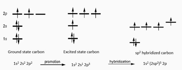
To kindle some technical minds, the reason for the mechanical strength and electronics property come from the sp 2 hybridization. It takes 6 electron to make a carbon atom and they are arranged as 1s2 2s2 2p2 and one graphene ring have 6 carbon atoms. So when two carbons atoms come together to form a molecule there forms an s-s covalent bond, and s – p sharing to form a sp 2 hybridization. The mechanical strength arise from the s-s covalent bond and the high conductivity comes from the hybridization.
In the case of silicon, the system is highly preferable for electronics because of its band structure properties. Silicon has an electronic configuration of [] 3s²3p² and two silicon atoms form a molecule with the p orbitals having a band structure as in Fig.3, here the gamma (Г) point on the left side, is the conduction band (where if an electron falls, have multiple position to move around and hence conducts electricity) while the fully filled Г’ point is the valance band (VB) where the electron stays stable and then gets excited to the conduction band (CB) when excited by the appropriate energy. The energy to be supplied is the energy difference between Г- Г’ which is the band gap. This crudely qualifies silicon to be a dielectric material. This band gap provides high amount of control between ON and OFF state of silicon. In the case of metals, Г and Г’ overlaps and hence needs no excess energy to move around from VB to CB, this means metals conducts in the ON state throughout.
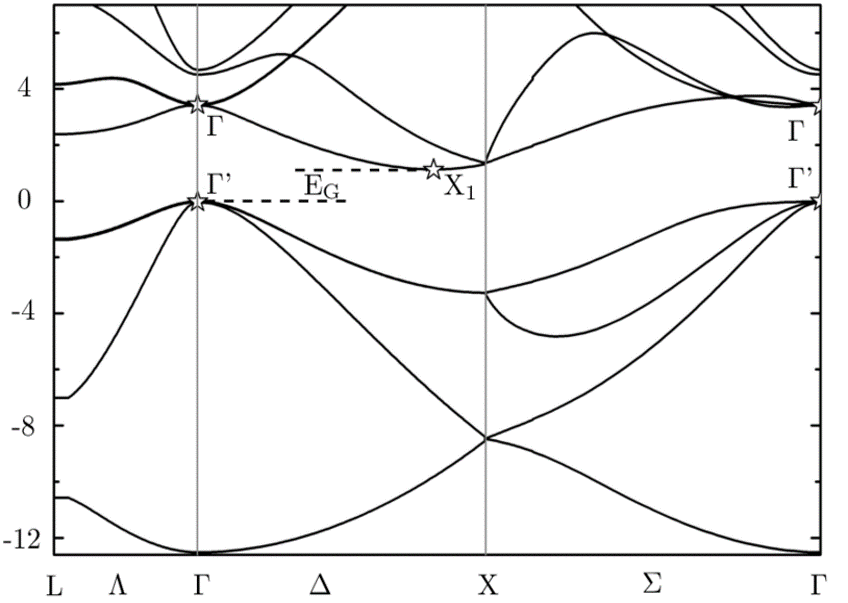
Fig.3. Band diagram of crystalline silicon with the x-axis is wave vector and y-axis is energy.
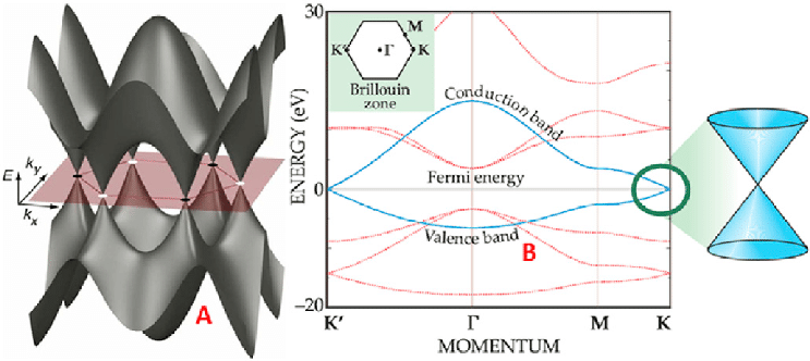
In the case of graphene, the conduction p band and the valence p band of graphene meet exactly at the corners of the hexagonal first Brillouin zone (Fig.4), these corners are called the Dirac points. Three of them, labeled as K, belong to one triangular sub lattice in reciprocal space, while the other three, labeled as K 0 , form the second sub lattice. The valence and conduction bands meet at the K and K 0 points, but do not overlap, with zero number of states just at these points. Because of this, graphene is called a zero band-gap semiconductor or semimetal. This band gap can be controlled for graphene by introducing an external electricity source (gate voltage) which enables graphene to act within a broad spectrum of conduction with the lower point being an insulator and the highest being a great conductor.
There have been concept cars with graphene roof which are used for solar power transporting, also we can think about coating the window glass with graphene layer so that they will be responsive to our commands and also stronger than the usual. The material is open for conversation because of which; making a composite with it is like eating a cake, a mix of concrete and graphene applied to a building can make the whole structure a smart building which needs no wires to strangle, no people movement to make life alive, no broken patches to hide and no thought about where the tv screen should be place- it is placed everywhere isn’t it, imagine the newspaper from harry potter movie becoming a reality, now that’s something I will really want!! .The idea of small and efficient high frequency (terahertz) detectors and antennas which are very much useful for high speed communication and internet services are possible with graphene.
It takes hundreds of years to understand most of ours handwriting, and so it is not a crime to take time in understanding the material that have been helping us in writing. Now we are in that hundred and one’ th year- intake innovate and initiate with graphene.
Note: All the pictures used in this article have been randomly collected from different website and papers and are not created by Nerdities.tech.

Innovating and insightfull.
LikeLike